

Serial Buses - An Established Design Standard
High-speed serial bus architectures are the new norm in today's high-performance designs. While parallel bus standards are undergoing some changes, serial buses are established across multiple markets - computers, cell phones, entertainment systems, and others and offer performance advantages, lower cost, and fewer traces in circuit and board designs and layouts.
You might already have experience with first and secondgeneration serial bus standards, like 2.5 Gb/s PCI Express® (PCIe) and 3 Gb/s Serial ATA (SATA). Engineers are now looking at the requirements in designing to third-generation specifications, including PCI Express 3.0 (8 Gb/s), that are still evolving in working groups.
Serial buses continue to advance with faster edge rates and a narrower unit interval (UI), creating unique, exacting demands on your design, compliance testing, and debug processes. Standards have reached speeds at which you need to be ready for RF analog characteristics and transmission line effects that have a far bigger impact on the design than in the past.
Faster transition times, shorter UIs, different pathway impedances, and noise sources in the amplitude domain all contribute more to bit error rate and add up to engineers needing to take a fresh look at their strategies for connectivity, pattern generation, receiver-side testing, data acquisition, and analysis. Coupling these issues with evolving standards and tighter compliance testing requirements creates a tougher job for companies to quickly get their products to market.
In this primer, we look at the compliance requirements of serial standards, with focus on the issues of next generation standards. After introducing the characteristics of several key standards, we'll look at the issues you face, including basic tests, and what you need to consider during the compliance testing and debug phases. We'll address five main areas: connecting to the device under test (DUT), generating accurate test patterns, testing receivers, acquiring data, and analyzing it.
A Range of Serial Standards
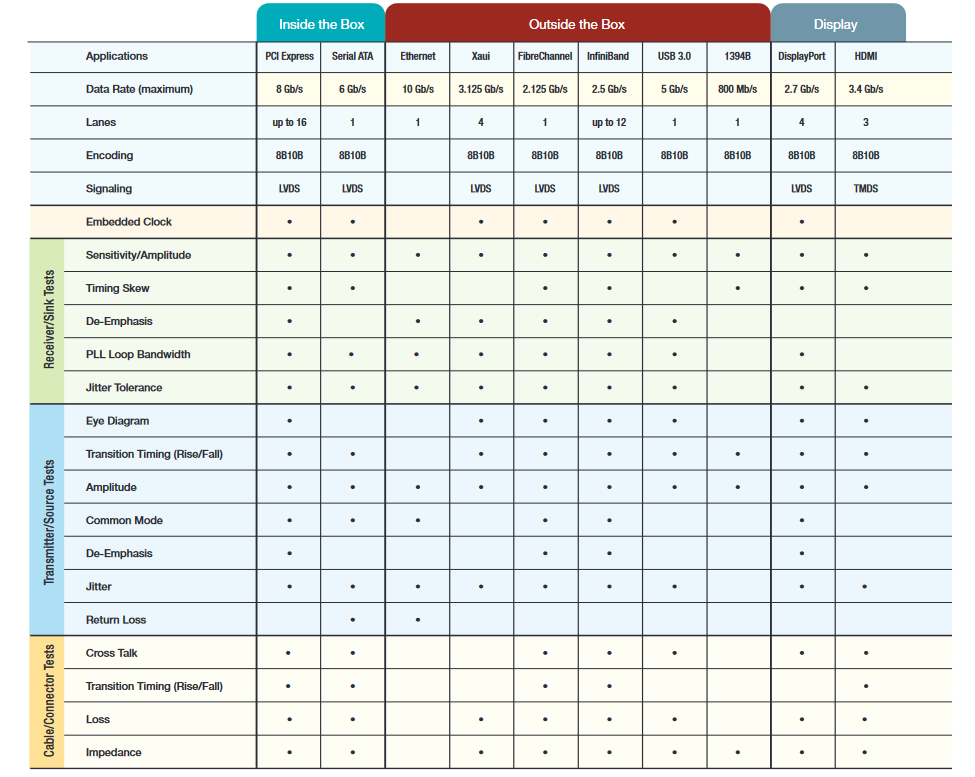
Across the electronics industry, manufacturers and other companies have introduced serial bus standards for multiple purposes to address the needs of their markets and customers. A key objective of the standards is to enable interoperability within an architecture across a wide range of products offered by a host of vendors. Each standard is managed by a governing body with committees and working groups to establish design and testing requirements. Table 1 lists some of the key serial standards.
Each specification defines attributes that products must comply with to meet the standard's requirements, including electrical, optical (if applicable), mechanical, interconnects, cable and other pathway losses, and many others. The governing body issues standardized tests that products must pass for compliance to the standard. The tests might be detailed to the point of requiring specific test equipment, or they might be more general and allow the designer/manufacturer to determine appropriate characteristics to be compliant. Specifications undergo change as the standards evolve. You must keep current your knowledge of the specification's requirements.
Tektronix is involved with many standards organizations and participates along with other companies in different working groups to help governing bodies establish effective testing processes and procedures for compliance testing.
In this document, we'll refer to the following three standards. Tektronix is involved in working groups in each of these standards.
SATA/SAS
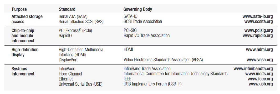
SATA is a serial standard for attached storage, widely used in today's desktop PCs and other computing platforms. It was initially released at 1.5 Gb/s, then was increased to 3 Gb/s with second generation (Gen2). Third generation SATA (6 Gb/s) devices recently entered the market. Serial Attached SCSI (SAS), like SATA, is a serial standard for storage applications. SAS designs, however, are primarily used in data center and enterprise applications. SAS operates at 3 Gb/s and SAS2 doubles that rate to 6 Gb/s.
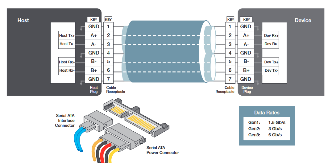
Figure 1 illustrates the SATA signals and mechanical layout. Like many serial standards, SATA and SAS uses lowvoltage differential signaling (LVDS) and 8b/10b encoding. Data travels between transmitters and receivers over dual-simplex channels; the link consists of one lane of transmit and receive pair. SATA uses a spread-spectrum clock (SSC) in an embedded clocking scheme without a separate reference clock transmitted to the receiver.
PCI Express®
PCI Express has replaced PCI in most chip-to-chip applications, including pathways crossing circuit boards and cable connections. PCIe is a highly scalable architecture, providing from one to 16 dual-simplex lanes in a PCIe link. In multi-lane applications, the data stream is divided up amongst the available lanes and transmitted nearly simultaneously at the lane rate. The fastest PCIe applications are typically used in graphics, connecting 16 lanes of high-speed, high-resolution graphical data between a system's chipset and a graphics processor. Figure 2 illustrates the PCI Express architecture.
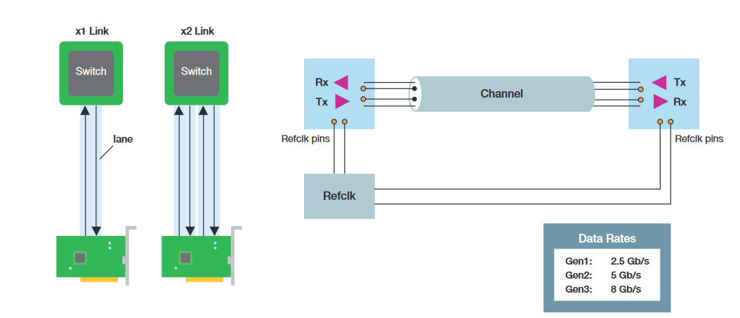
The first-generation per-lane transfer rate for PCIe is 2.5 Gb/s with PCIe 2.0 providing 5 Gb/s rates. Soon there will be products with 8 Gb/s transfer rates for PCIe third generation. PCIe embeds the clock in the data stream, but also couples a reference clock to drive the PLL reference input on the receiver.
Ethernet
Ethernet is a Local Area Network (LAN) technology defined by the IEEE 802.3 standard and is a widely adopted standard for communication between multiple computers. Ethernet interfaces varies from application to application and includes both electrical (twisted-pair cable, copper backplane) and optical (multimode fiber) signaling media. Currently the most popular Ethernet interface is Unshielded Twisted Pair (UTP).
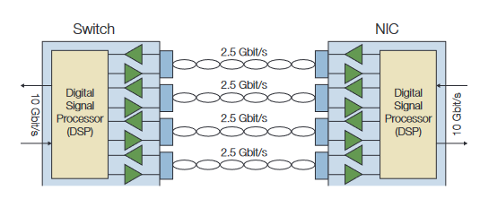
First and second-generation Ethernet standards, 10BASE-T and 100BASE-T, provide a transfer rate of 10 Mb/s and 100 Mb/s respectively. Broad deployment of Gigabit Ethernet (1000 Mb/s) is under way with 10GBASE-T designs emerging soon. The 10GBASE-T specification employs full duplex baseband transmission over four pairs of balanced cabling. The aggregate data rate of 10 Gb/s is achieved by transmitting 2500 Mb/s in each direction simultaneously on each wire pair as shown in Figure 3.
USB
Universal Serial Bus has become known as the de facto standard for connecting personal computers and other peripheral devices. USB 2.0 (480 Mb/s) was adopted in 2000 with 40x speed improvement over the legacy USB 1.1 (12 Mb/s) specification. Recently the USB 3.0 or SuperSpeed USB specification was introduced at a 10x improvement over USB 2.0. With a 5 Gb/s data rate SuperSpeed USB will accommodate data-intensive applications like High Definition video and fast I/O to flash memory devices. Because of the large adoption of legacy USB products USB 3.0 provides complete backwards compatibility. Figure 5 shows the link architecture for SuperSpeed USB.
HDMI/DisplayPort
The High Definition Multimedia Interface (HDMI) is the first specification designed specifically to address the needs of the consumer entertainment systems market. HDMI builds on the highly successful Digital Video Interface (DVI) for PCs and extends it with additional capabilities for home entertainment devices, like large-screen, high-definition TVs and home theater systems. Figure 4 illustrates the HDMI architecture.
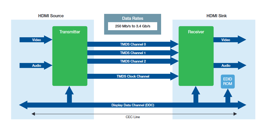
HDMI transmits high-resolution video and multi-channel audio from a source to a sink. The specification defines three data channels in the HDMI link with transmission rates from 250 Mb/s to 3.4 Gb/s, depending on the display resolution.
While most high-speed serial standards rely on LVDS with 8b/10b encoding, HDMI uses transition-minimized differential signaling, or TMDS, to reduce the number of transitions on a link and minimize electromagnetic interference (EMI).
HDMI also uses a reference clock transmitting at 1/10th the data rate. A low-speed serial bus (I2C), called the DDC bus, exchanges configuration and identification data bi-directionally between the source and sink.
The DisplayPort specification defines a scalable digital display interface with optional audio- and content-protection capability for broad usage within business, enterprise, and consumer applications. The interface is includes support for two data rates: Reduced Bit Rate (1.62 Gb/s) and High Bit Rate (2.7 Gb/s).
Common Architectural Elements
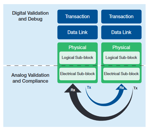
All the high-speed serial standards follow a layered model, as illustrated in Figure 6. The Physical layer comprises an electrical and logical sub-block. This primer focuses on the electrical sub-block, where electrical compliance testing is completed.
Many high-speed serial standards incorporate the same or similar architecture elements at the electrical level, such as:
- Differential signaling (LVDS or TMDS) for high data rates and high noise immunity
- 8b/10b encoding to improve signal integrity and reduce EMI
- Embedded clocks and some with reference clocks
- Spread-spectrum clocking to reduce EMI
- Equalization to compensate for signal attenuation from lossy channels
- Typical measurements include jitter, amplitude, differential skew, risetime/falltime, and common mode
- Specifications and testing requirements evolve as more insight is gained and the standards advance
Table 2 lists some of the architecture's key elements and compliance tests.
Differential Transmission
Differential transmission has been a part of communications technology since the early days of telephone networks. A differentially-transmitted signal consists of two equal and opposite versions of the waveform traveling down two conductors to a differential receiver1. When the signal on one leg of the differential path is going positive, the signal on the other leg is going equally negative, as shown in Figure 2. These two mirror images of the signal combine at the destination. Differential techniques resist crosstalk, externally induced noise, and other degradations. Properly designed and terminated, a differential architecture provides a robust path for sensitive high-frequency signals.
8b/10b Signal Encodin
Many serial standards employ 8B/10B encoding, an IBM patented technology used to convert 8-bit data bytes into 10-bit Transmission Characters. These Transmission Characters improve the physical signal to bring about several key benefits: bit synchronization is more easily achieved; the design of receivers and transmitters is simplified; error detection is improved; and control characters (such as the Special Character) can be more readily distinguished from data characters.
Embedded Clocks
Many (if not most) current serial devices rely on embedded clock signals to maintain synchronization between transmitting and receiving elements. There is no separate clock signal line; instead, the timing information resides in the data signal. As we will see later in this document, this imposes certain requirements on the data signal. Encoding methods such as 8b/10b are used to guarantee that usable reference edges occur regularly enough to provide the needed synchronization.
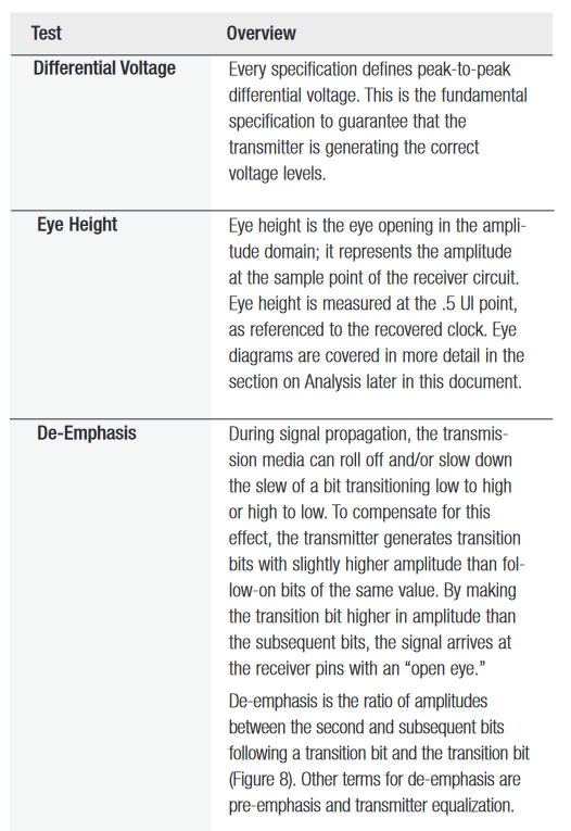
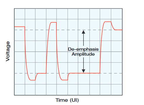
De-Emphasis
A technique known as de-emphasis modifies certain bits in a given sequence. That is, the first bit following a series of bits having the opposite state is higher in amplitude than subsequent bits. These subsequent bits, then, are de-emphasized. The purpose of this practice is to counteract frequency dependent losses in transmission media such as FR4 circuit boards.
Low Voltage Signaling
Modern serial architectures that employ differential transmission also use low-voltage signaling. Not surprisingly, the approach is known as Low Voltage Differential Signaling, or LVDS. Fast buses often rely on very low-voltage signals simply because it takes less time to change states over the span of a few hundred millivolts, for example, than it takes to make a full one-volt transition. Outwardly this might seem more susceptible to interference and noise, but differential transmission protects against such effects.
Next-generation Serial Challenges
At the data rates next-generation serial standards operate, analog anomalies of the signal have a greater impact on signal integrity and quality than ever before. Conductors in signal pathways, including circuit board traces, vias, connectors, and cabling, exhibit greater transmission line effects with return losses and reflections that degrade signal levels, induce skewing, and add noise.
Gigabit Speeds
With each increase in transfer rates of the standards, the UI shrinks, and the tolerances in transmitter signal quality and receiver sensitivity become tighter. Low-voltage differential signals and multi-level signaling are more vulnerable to signal integrity issues, differential skew, noise, and inter-symbol interference (ISI) as speeds increase. There is greater susceptibility to timing problems, impedance discontinuities between a transmitter and receiver, and system level interaction between hardware and software. Multi-lane architectures amplify design complexity and potential for lane skew timing violations and crosstalk.
Jitter
Today's higher data rates and embedded clocks mean greater susceptibility to jitter, degrading bit error rate (BER) performance. Jitter typically comes from crosstalk, system noise, simultaneous switching outputs, and other regularly occurring interference signals. With faster rates, multi-lane architectures, and more compact designs, there are more opportunities for all these events to affect data transmission in the form of signal jitter.
Transmission Line Effects
The signal transmitter, conductor pathways, and receiver constitute a serial data network. Buried in that network are distributed capacitance, inductance, and resistance that have diverse effects on signal propagation as frequencies increase. Transmission line effects rise from this distributed network and can significantly impact signal quality and lead to data errors.
Noise
Noise is unwanted aberrations in the amplitude domain that appear in the signal. Noise comes from both external sources, such as the AC power line, and internal sources, including digital clocks, microprocessors, and switchedmode power supplies. Noise can be transient or broadband random noise and can lead to phase errors and signal integrity problems. Like jitter in the frequency domain, with faster signaling, noise in the amplitude domain adds variations that can have a critical impact on BER performance.
Compliance Testing
Serial standards normally include amplitude, timing, jitter, and eye measurements within their compliance testing specifications. The latest versions of some standards add focus, compared to previous versions, on SSC clocking, receiver sensitivity testing, and measurement of return loss and reflections on connectors, cables, and other pathways. Not all measurements are required for compliance with every standard.
Test points are specified in the standard's compliance test document or the specification itself.
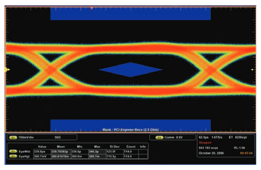
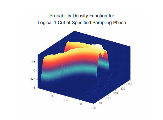
Eye Measurements
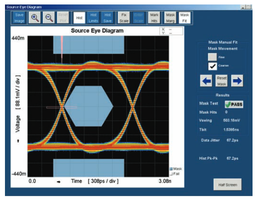
Key compliance verification comes from eye measurements. An eye diagram is shown in Figure 7. Eye measurements result from superimposing multiple, one unit interval (UI) signal captures (the equivalent of one clock cycle) of the data stream, triggered to the recovered clock. Failure zones in the middle of the eye and above and below the eye are typically indicated by a "mask" (blue areas), showing the boundaries the test must not violate. Eye measurements are further discussed in the Analysis section later in this document.
The following tables encapsulate some of the key measurements commonly required at plug-fests (to prove compliance and interoperability) and ultimately, in certified compliance verification procedures.
Amplitude Tests
The amplitude tests listed in Table 3 verify that the signal achieves the voltage levels and stability to reliably propagate through the transmission media and communicate a proper "one" or "zero" to the receiver.
Timing Tests
The timing tests listed in Table 4 verify the signal is free from excess timing variations and its transitions are fast enough to preserve the critical data values the signal is meant to deliver. These tests, which require uncompromised performance on the part of the measurement toolset, detect aberrations and signal degradation that arise from distributed capacitance, resistance, crosstalk, and more.
Jitter Tests
With faster data rates, jitter becomes one of the most difficult issues to resolve, which is one reason jitter measurements continue to be a topic of extensive discussion in standards bodies' working groups. It is also a focus of companies that develop specialized analysis tools to help you quickly identify the causes and results of jitter and to understand this complex issue.
Jitter is a result of spectral components, both deterministic and random. To guarantee interoperability, the transmitter must not develop too much jitter, and the receiver must be able to tolerate a defined amount of jitter and still recover the clock and de-serialize the data stream. Other signal characteristics, such as amplitude and rise time can affect any jitter tolerance property. In effect, jitter is a bit error ratio measurement and is usually quantified in terms of total jitter at a specified bit error ratio (BER).
Time interval error (TIE) is the basis for many jitter measurements. TIE is the difference between the recovered clock edge (the jitter timing reference) and the actual waveform edge. Performing histogram and spectrum analysis on a TIE waveform provides the basis for advanced jitter measurements. Histograms also help you isolate jitter induced by other circuits, such as switching power supplies.
Jitter measurements generally require long test times, since they must record literally trillions of cycles to ensure an accurate representation at 10-12 BER performance. An oscilloscope with high capture rate and jitter analysis tools can reduce test times for these jitter tolerance tests. See the Analysis section later for more details about jitter measurements.
Receiver Sensitivity Tests
The governing bodies of some standards have focused more on receiver sensitivity testing in their latest test specifications. Receiver sensitivity verifies the ability of the clock-data recovery (CDR) unit and de-serializer in the receiver component to accurately recover the clock and the data stream under certain adverse signal characteristics, including jitter, amplitude, and timing variations. This area of testing is covered in more detail in Receiver Sensitivity Testing below.
Circuit Board and Interconnect Tests
The transmission media play an increasingly critical role in signal quality. An LVDS signal running at multi-gigabit data rates through a low-cost medium, such as FR4, plus connectors and cables, poses many layout challenges in both product and test fixture design and testing. Many standards require a more critical look at characterizing media with loss, impedance, crosstalk testing, and eye analysis.
Compliance Testing Solutions
Getting the right signal with minimal impact from the measurement system is paramount in evaluating performance of a new design. Five areas are critical to the testing process:
- Connectivity
- Pattern Generation
- Receiver Testing
- Acquisition
- Analysis
Connectivity
Measurement pathways, including the DUT-to-oscilloscope path, have transmission line effects and can lead to degraded signals and test failure. Proper connectivity with the correct probe is essential.
The mechanical portion of the standard, sometimes called the physical media dependent (PMD) specification, often determines how to connect to the DUT. With many standards, you will find diverse configurations, each with its own unique characteristics.
There are five approaches to the probing challenge:
- TriMode™ differential probes enable single-ended and differential measurements from a single setup on a test point
- SMA pseudo-differentially connected probes for connecting to fixtures
- True differential movable probes for direct, differential measurements
- SMA true differential probes for connecting to fixtures
It is important to note that any probe will impose some loading on the Device Under Test (DUT). Every probe has its own circuit model whose impedance can change with increasing frequency. This can affect the behavior of the observed circuit and influence the measurement, factors that must be considered when evaluating results.
TriMode™ Differential Probes
TriMode probes change differential probing by enabling single-ended, differential, and common mode measurements with a single connection to the DUT.
Traditional measurement methods require two single-ended probes for common mode measurements, plus a differential probe setup for true differential signal acquisition (Figure 9a). TriMode probes accomplish both setups with a single probe (Figure 9b).
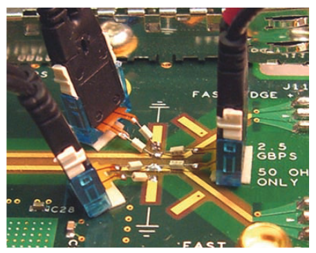
Pseudo-differentially Connected Movable Probes
Troubleshooting work may require probing circuit points anywhere on a device's circuit board. This makes it necessary to probe individual circuit traces and pins with movable probes. Two single-ended active probes, one on each side of the differential signal, can be used for pseudo-differential measurements and common-mode measurements. Figure 10 illustrates this type of connectivity.
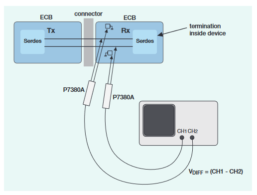
Two channels of the oscilloscope capture two channels of data, which are subsequently processed as one signal, resulting in a math waveform. Because the two sides of the waveform enter two separate oscilloscope input channels, the inputs must be deskewed before making any measurements to eliminate instrument impacts on the acquisition.
SMA Pseudo-differentially Connected Probes
Many compliance test fixtures and prototype circuits are fitted with SMA high-frequency connectors for external test instrumentation. Under these conditions, the SMA pseudo-differential approach is a practical solution. Here the output of the transmitter connects directly to two inputs of the oscilloscope, each with an input impedance of 50Ω. SMA adapters provide the necessary mechanical termination on the front panel of the oscilloscopes.
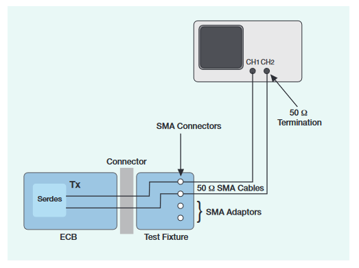
As explained earlier, this pseudo-differential technique consumes two channels of the oscilloscope, and probe deskewing is critical. Figure 11 illustrates this kind of fixture connectivity.
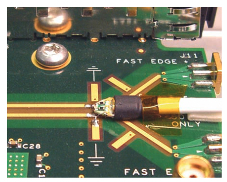
True Differential Movable Probes
A true differential active probe is optimized as a low-loss, high-fidelity path for differential signals. Figure 12 shows such a probe capturing the receive side of a connectorbased card-to-card serial link.
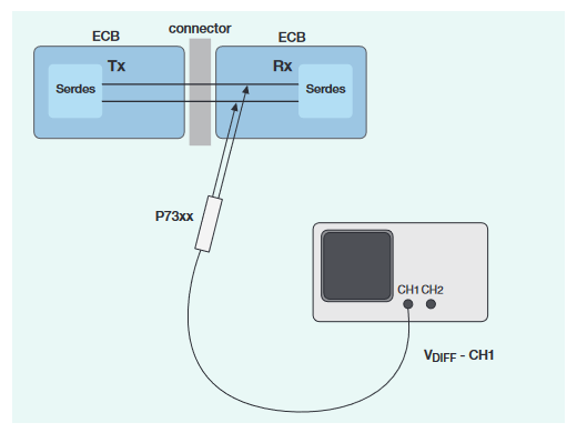
Unlike the pseudo-differential connection, this probe requires only one oscilloscope channel and makes the subsequent math steps unnecessary. This offers, among other advantages, the ability to use several channels of the oscilloscope to simultaneously capture multiple lanes at the highest sample rates. It is also useful for debugging multiple high-speed test points.
SMA True Differential Probes
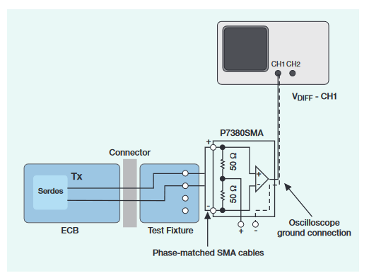
The SMA input differential probe is also ideal for compliance tests where interoperability points are defined at the card-to-card or card-to-cable interface. A 100Ω matched termination network properly terminates both legs of the differential signal to any user-provided common mode voltage. The voltage may be at ground potential or a termination voltage appropriate to the logic family being tested. The common mode connector can also be left open if the transmitter will drive a 100Ω differential load. Figure 13 illustrates a true differential SMA probe attached to a card-to-card interface and fixture.
Fixtures
Like all other aspects of serial architectures, increased data rates can have a significant impact on test fixtures. You must qualify any existing fixtures under the new standards to ensure they continue to deliver a correct signal to the measurement system. With the faster rates for PCI Express and SATA, the impact on existing fixtures is notable, and requires redesign and new board layouts.
In some cases, low cost media, such as FR4, are no longer suitable for new designs based on second- and third-generation serial architectures. These media present too many losses and returns to adequately propagate a signal and maintain proper signal integrity. You might need to evaluate newer, more expensive materials. In some cases you may need to incorporate additional equalization techniques such as receiver equalization to overcome signal loss.
Pattern Generation
Each standard's test document specifies the "golden" pattern that must be applied to the DUT for compliance verification. This specified pattern is critical to achieve the desired results.
In some cases, like PCI Express, the transmitter/receiver generates its own test sequence. Other standards require more complex handling of the signal, possibly with help from a host processor.
When an external signal is required, the test equipment must generate the golden pattern at the right frequency and with all the necessary characteristics to adequately test the device according to the test specification. The right tool for this is the programmable signal source, including:
- Data timing generators that offer standard test signals, such as TS1 and TS2 training signals and Pseudo-random bit streams (PRBS)
- Arbitrary waveform generators that provide highly definable real-world signals along with digital patterns
- Jitter sources that vary input signals for stress testing
- New all-in-one signal generators that simplify testing with analog waveforms, digital patterns, and signal sources to vary outputs with diverse modulation schemes
To automate the testing process, connectivity between other test instruments, such as oscilloscopes, logic analyzers, and PCs, helps accelerate compliance verification. Programmability using math waveforms generated from applications like Matlab, and the ability to capture and re-generate waveforms can also speed testing.
Receiver Sensitivity Testing
The receiver is at the end of a possibly diverse transmission path. Yet, it must interoperate with the many different transmitters connected through various interconnects, each with its own effect on the signal.
In order to guarantee interoperability, the receiver section, particularly the clock-data recovery (CDR) unit and de-serializer, must operate correctly under a broad range of conditions. The CDR must extract the clock in the presence of variations in jitter and amplitude. Similarly, the de-serializer must tolerate a specified amount of amplitude, jitter, and skew to comply with a particular standard.
The Test Process
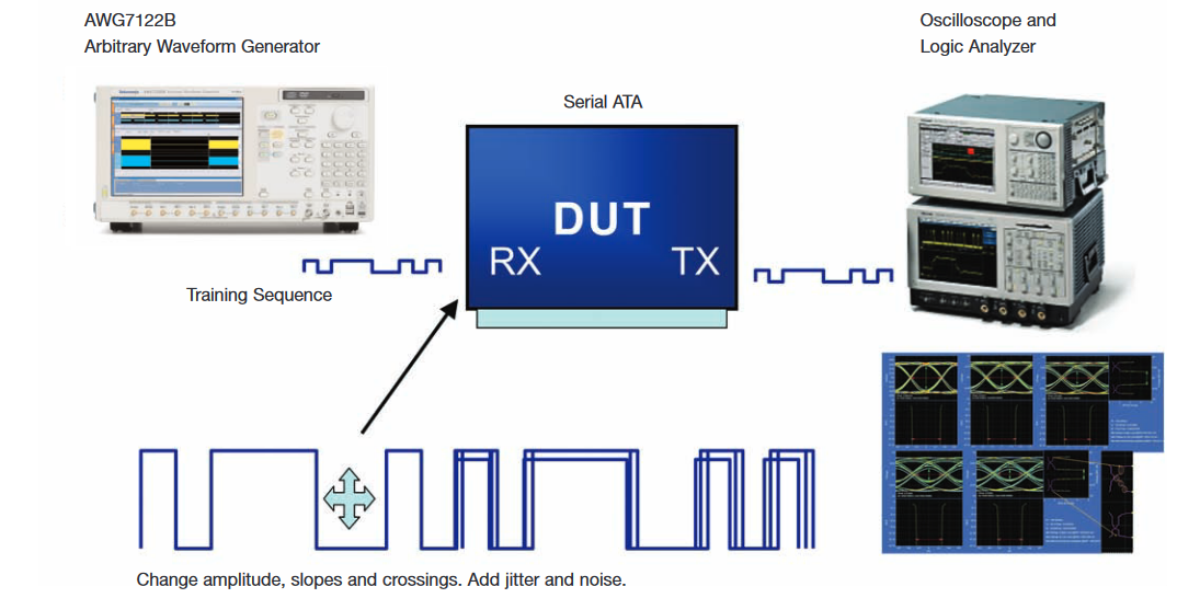
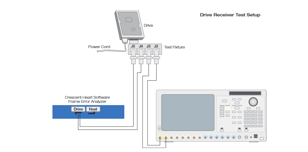
Figure 14 illustrates a single-lane SATA receiver test setup. While the exact test parameters, procedures, and tolerances vary among standards, the basic test methodology comprises the following:
- Set the device to loopback mode and monitor the transmitter output with a logic analyzer and/or oscilloscope, serial bus analyzer, or error detector to check that the transmitted pattern is the same as the test pattern
- Insert the specified golden test pattern
- Vary the amplitude to make sure the receiver can accurately recognize 0 and 1 values
- Vary the skew between differential pairs to allow for tolerances in board layout and cabling
- Insert jitter to make sure the CDR phase-locked loop (PLL) can track the input
Seeing Inside the Receiver
The difficulty with receiver testing and debugging is that you cannot directly probe the signal within the device to debug problems. Many receivers are designed with input filters that compensate for transmission line losses and effects, delivering a "clean" signal to the CDR. So, an oscilloscope probe at a receiver's input pins sees the signals before the filter is applied.
Advanced oscilloscopes with programmable DSP filtering techniques enable you to acquire signals at "virtual test points" within the receiver to view signal characteristics after filtering. By applying the input filter coefficients to the oscilloscope's Math system, the oscilloscope displays the signal characteristics beyond the input filter and any equalization that may be applied. This reveals more accurate eye testing at the CDR input where clock recovery and equalization are accomplished and jitter has its impact. Note in Figures 15a and 15b the difference in results of eye measurements due to FIR filtering.
Receiver Amplitude Sensitivity Measurements
Signal losses are inevitable before reaching the receiver. Amplitude sensitivity measurements check that the receiver can accurately recognize the proper bit value once the signal reaches the CDR and de-serializer.
Receiver Timing Measurements
Timing tests vary the skew of the differential pair and edge rates to verify the receiver's tolerance of changes in signal timing. Differential outputs on the pattern generator or arbitrary waveform generator providing the test signals are essential.
Receiver Jitter Tolerance Measurements
Jitter tolerance for receivers is defined as the ability to recover data successfully in the presence of jitter and noise. Meeting the specification guarantees that the CDR can recover the clock and place the data sample strobe in the center of the UI. It also means that the de-serializer can recognize the data, even when a certain amount of jitter is present. Figure 16 illustrates a receiver jitter measurement setup.
Rigorous jitter tests are especially critical in applications such as SATA, in which the clock is embedded in the 8b/10b-encoded data stream. The waveform generator must be able to supply jitter with specific amplitude and frequency modulation profiles, such as sine wave, square wave, triangle wave, and noise. To adequately stress the device under conditions it might encounter, the generator must also be able to apply jitter to either or both the rising or falling edge.
Inter-symbol interference (ISI) in receiver testing is a topic of rising interest in working groups. Engineers and researchers are examining the effects of ISI on the receiver and how to best test and characterize the effects as signal rates increase. Standards such as DisplayPort and HDMI have incorporated cable emulator models for jitter tolerance testing emulating a worse case ISI model.
Signal Acquisition
Characteristics of the measurement equipment can result in non-compliance of a device that is working properly. The acquisition system – probes, cables, and oscilloscope input together – must be adequate to pass enough information during acquisition to make accurate measurements. Key to good acquisition are:
- Bandwidth
- Adequate Number of Inputs
- Sample rate
- Record length
Bandwidth Requirements
Most first-generation serial bus architectures use date rates from 1.5 Gb/s to 3.125 Gb/s, yielding fundamental clock frequencies as high as 1.56 GHz. These rates are within reach of 4 and 5 GHz oscilloscopes. But signal fidelity measurements and accurate eye analyses demand much higher bandwidth. Most standards bodies recognize this need.
Bandwidth requirements go up with second and third generation standards (and beyond), with data rates as high as 10 Gb/s.
Bandwidth and Transitions
Often, the rise-time requirements for a standard are more demanding on bandwidth than the data rates. Table 5 lists bandwidth requirements needed for various risetime measurement accuracies at risetimes found in today's standards.
Both the oscilloscope's and probe's transition times affect the signal's measured risetimes and falltimes. The equation below shows the relationship between the probe/oscilloscope system, signal, and displayed risetime measurements. The probe and oscilloscope must be considered as a system and removed from the displayed measurement to arrive at the signal's true risetime.
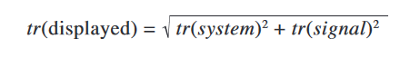
For example, a system with a 20% to 80% risetime specification of 65 ps, when applied to a signal with a true risetime of 75 ps would display a measurement of 99 ps. This is an unavoidable measurement artifact of the system. Thus, it is desirable to minimize the impact of the measurement system whenever possible with a faster risetime specification for both the oscilloscope and probe.
Acquiring From Multiple Lanes
High data rates, low-cost media, and multiple lane designs with standards like HDMI can have adverse effects on inter-lane skew and crosstalk. An oscilloscope providing simultaneous real-time data capture across multiple lanes, with the performance necessary to service the latest generation of serial standards can speed and simplify testing, validation, and debugging.
With time-correlated, captured waveform data on multiple lanes you gain a better understanding of the context in which an error occurred. With HDMI, recording all lanes of time-correlated data provides insight into, not only the offending event, but also the events that preceded and followed it on every lane.
Sample Rate and Record Length
Along with adequate bandwidth to capture signal characteristics, an oscilloscope must store enough waveform information (record length) with enough detail (sample rate) at the required bandwidth to complete the standardized tests. Each standard specifies the minimal amount of data to capture to complete a test. Of course, more data with greater detail affords deeper analysis into signal anomalies that might occur over longer time periods. Advanced oscilloscopes, with longer record lengths, faster sampling rates, and wider bandwidth, can use these features to their advantage and your benefit, to present a higher degree of analysis.
Along with adequate bandwidth to capture signal characteristics, an oscilloscope must store enough waveform information (record length) with enough detail (sample rate) at the required bandwidth to complete the standardized tests. Each standard specifies the minimal amount of data to capture to complete a test. Of course, more data with greater detail affords deeper analysis into signal anomalies that might occur over longer time periods. Advanced oscilloscopes, with longer record lengths, faster sampling rates, and wider bandwidth, can use these features to their advantage and your benefit, to present a higher degree of analysis.
Advanced oscilloscopes with long record lengths and builtin analysis tools can include proprietary analysis techniques that reveal greater detail about the signal over the entire acquisition, offering more confidence in the design. For example, while PCIe 1.0 requires a minimum sampling of 250 cycles for compliance verification, with a capture of 1 million cycles, advanced tools allow analysis of any contiguous 250 cycles throughout the record length to evaluate signal quality in more depth.
For multi-lane signal acquisition, record length and sample rate should apply across each lane in a multi-channel oscilloscope to ensure the greatest detail possible during acquisition.
Signal Analysis
The correct application of the right probes, the golden pattern applied to the DUT, and the best choice in the test instrument's acquisition system, help with a higher degree of confidence in the output of your analysis.
Automated measurement and analysis tools are commonly used to speed the selection and application of compliance tests. Oscilloscopes with automated analysis tools help accelerate and evaluate BER, eye opening, return loss, and reflection measurements. Advanced instruments offer new, unique approaches and techniques to perform deeper analysis and troubleshooting for greater confidence in design outcomes and faster isolation of problems.
Real-time or Equivalent-time Oscilloscopes
While most standards design their tests around real-time sampling oscilloscopes, and these scopes are most often used in compliance verification, other standards require equivalent-time (also called sampling) oscilloscopes. Each type has its own unique requirements and advantages.
Real-time (RT) oscilloscopes acquire an extended set of measurement data from a single trigger, and then perform measurement and analysis on the data. The amount and detail of data are limited by the oscilloscope's bandwidth, record length, and sample rate. Advanced instruments use software digital signal processing (DSP) to recover the clock, which means different clock recovery models can be quickly loaded to adapt to different tests. The real-time oscilloscope can acquire data from any type of input stimulus, whether it's a fixed, repeating pattern or a single anomaly
Equivalent-time (ET/sampling) oscilloscopes build up a waveform from samples of a repeating signal. These oscilloscopes can sample and "create" much faster signals than real-time oscilloscopes, but they require a repeating signal. The fastest oscilloscopes are typically ET systems. Sampling oscilloscopes rely on a hardware-based clock recovery unit that must trigger the system for every sample. It typically takes a much longer time to perform measurements, requiring many repeated acquisitions, but an advanced triggering system that speeds re-arm time for the trigger circuit helps shorten measurement times.
Modern, advanced sampling oscilloscopes also integrate time domain reflectometry (TDR) and time domain transmission (TDT) capabilities, and offer S-parameter-based modeling and analysis of circuits and transmission media. These features enable de-embedding of test equipment effects and circuit elements, plus advanced signal processing, to reveal more accurate signal characteristics and provide greater insight to causes of design challenges.
Eye Analysis
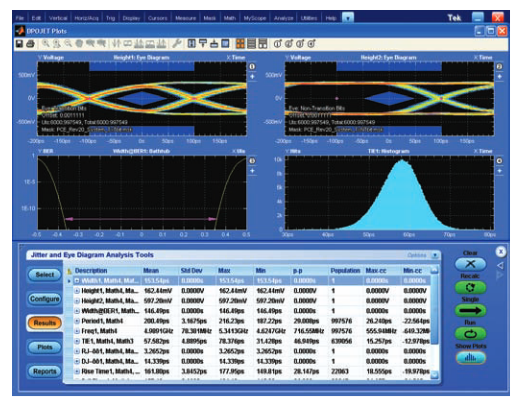
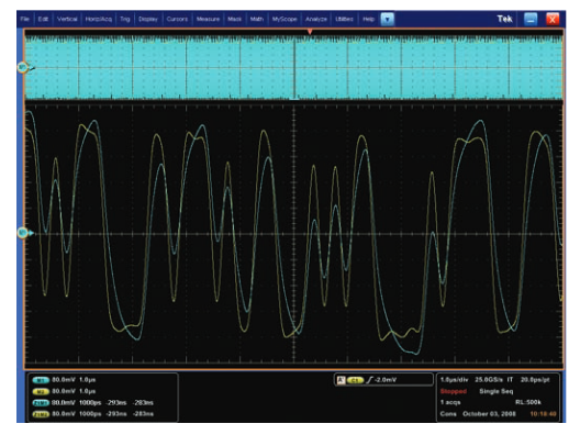
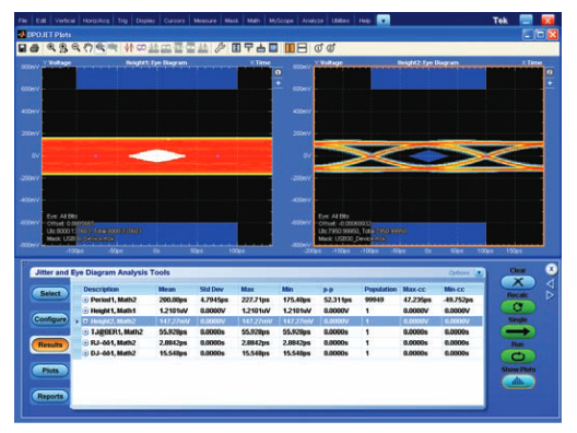
Each standard specifies how to capture data for eye measurements, including the clock recovery method, and the masks that determine compliance or non-compliance. In addition to the eye measurement display, oscilloscope analysis tools can perform statistical analysis to determine violation of mask boundaries and other critical parameters. Figure 17 shows an eye measurement of all edges, with and without de-emphasis, that passes the mask boundaries. This single measurement provides information about the eye opening, noise, jitter, and risetimes and falltimes.
Most standards place the mask in the center of the eye. HDMI, however, offsets the mask as seen in Figure 18. It's critical to understand the differences in eye measurement standards when working with different architectures.
Jitter Analysis
Jitter measures the difference between an expected signal edge, based on a golden clock model specified by each standard, and the actual edge recovered from the embedded clock. Too much jitter degrades BER performance.
Determining Jitter and BER Performance
Standards specify total jitter tolerance at 10-12 BER. Acquiring the necessary cycles to analyze jitter to this degree is prohibitively time-consuming, so standards bodies have devised measurements that accurately extrapolate to the 10-12 BER level.
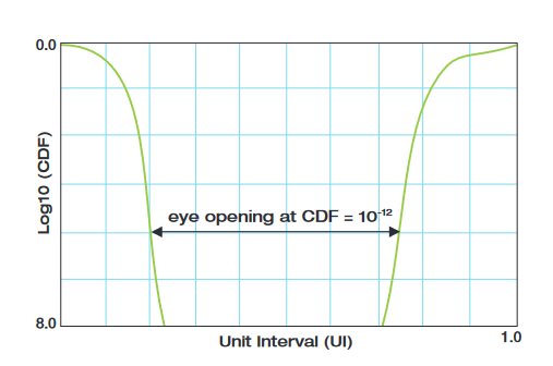
Different standards use different approaches for extrapolation. A common method is to use a cumulative distribution function (CDF), or bathtub curve (Figure 19) derived from TIE measurements. The InfiniBand standard uses this method. First-generation PCI Express relies on a TIE histogram, while second-generation PCI Express uses the Dual Dirac model (Figure 20).
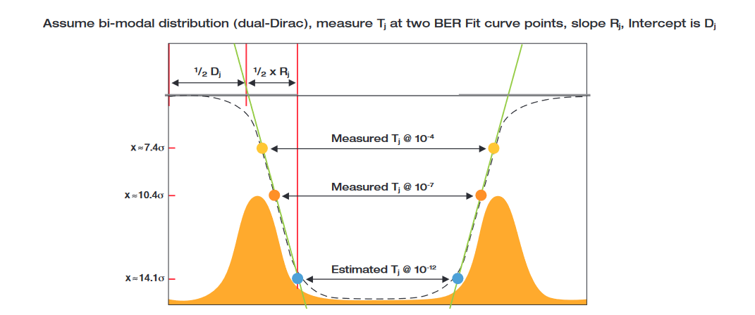
The amount of jitter at 10-12 BER is considered the jitter eye opening, which is different from the eye width of eye measurements. The relationship between Tj, jitter eye opening, and UI is as follows:
Total Jitter + Jitter Eye Opening = 1 Unit Interval
Total jitter (Tj) combines random (Rj) and deterministic (Dj) components from various sources, as illustrated in Figure 21.
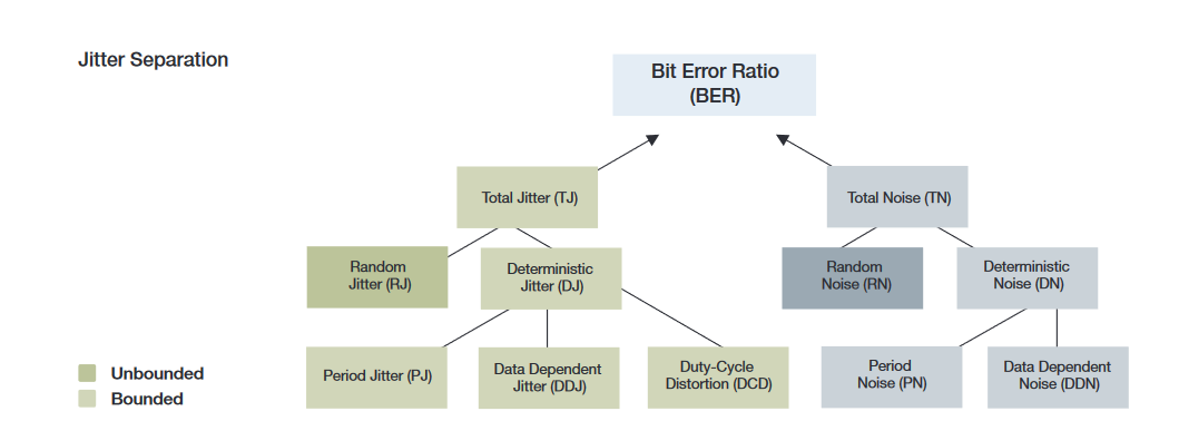
As shown in Figure 20, Dj and Rj can be measured from the CDF. Advanced real-time and sampling oscilloscopes integrate software toolsets for performing jitter measurements and for separating Rj and Dj. Under-standing Rj and Dj can help you isolate circuit components that contribute to jitter.
Not all jitter measurements are the same. A standard's clock recovery model drives its particular jitter measurements. This means automation tools have to incorporate the specific type of clock recovery method for a given standard to perform jitter measurements for that standard. Different methods can result in different jitter evaluation. So, it's critical you use the correct method and follow the test document's requirements. Programmable oscilloscopes for software-based clock recovery and hardware clock recovery systems for sampling oscilloscopes simplify this task.
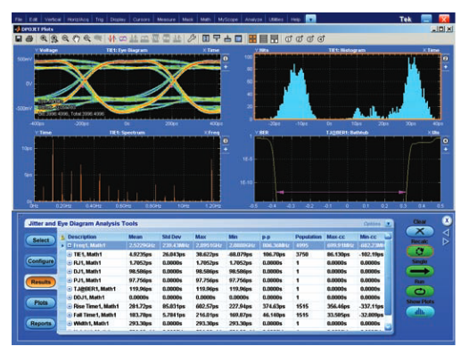
Proprietary tools also exist, integrated into advanced oscilloscope toolsets. These toolsets can offer an in-depth, comprehensive look at jitter and other measurements. Figure 22 shows multiple views of jitter analysis, including eye opening, TIE spectral analysis, and BER using the bathtub curve, in a single display. Statistical analysis indicates the results of different measurements, offering an instant decision about DUT performance and compliance.
The more data you can gather about jitter, the better your measurements for this all-important compliance test. Measuring low frequency jitter makes two conflicting demands on the oscilloscope: asking it to capture tiny timing details and to do so over long spans of time. To accomplish this, the oscilloscope must have both high sampling rates to acquire maximum detail about each cycle, plus a long record length to analyze low-frequency changes over time. Modern oscilloscopes with up to 50 Gs/s sampling rate and a very deep memory allow the instrument to capture enough operational cycles to determine the impact of low frequency jitter on the measurements.
Noise Analysis
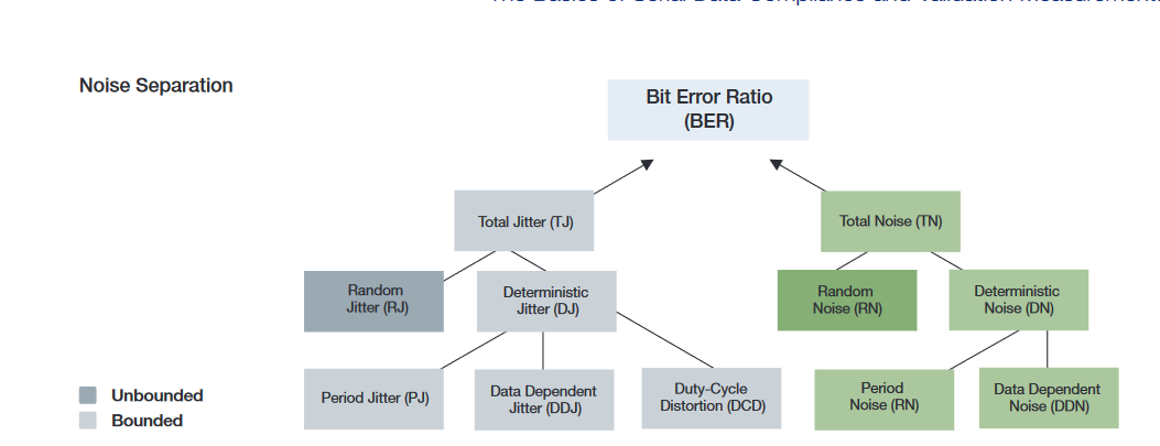
As data rates increase and tolerances get tighter, higher measurement accuracies will require even greater diligence in reducing the effects of vertical noise in the amplitude domain. Since amplitude noise and timing jitter are not orthogonal, the manifestation of amplitude variations as phase error must be accounted for. The noise model follows a distribution similar to jitter, with both random and deterministic components (Figure 23), which can be modeled by a noise separation image (Figure 24).
SSC Analysis
Many standards use spread spectrum clocking to reduce EMI. These standards require verification of the SSC profile against the specifications. Again, with high sample rates and long record lengths, statistical analysis can reveal the low-frequency variations across an acquisition of hundreds to millions of cycles.
Transmission Media Analysis
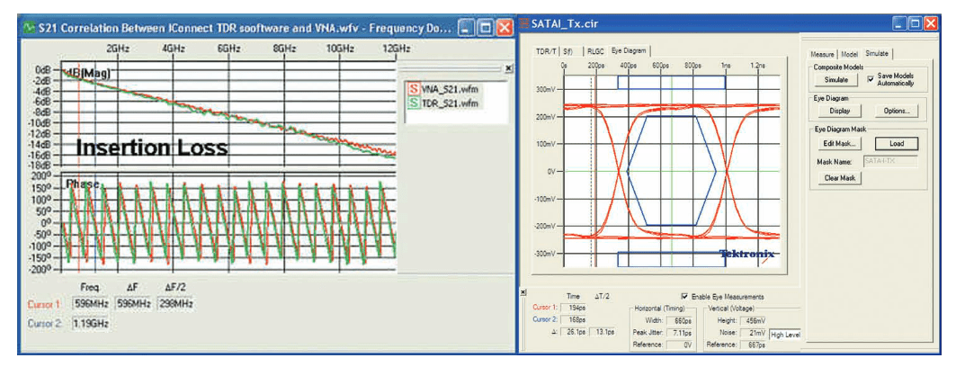
Accurate analysis of signal paths and interconnects in both time and frequency domains is critical to fully understand the effects of loss and crosstalk in today's high-speed serial designs. Industry standards, such as PCI Express and SATA, increasingly call for the use of S-parameters and impedance measurements to characterize signal path effects and ensure system interoperability. Advanced sampling oscilloscopes with TDR capabilities enable S-parameter-based modeling, return loss and eye measurements (Figure 25), and complex network analysis to verify compliance of cables and interconnects within a standard.
De-embedding/Normalization
S-parameter modeling of the measurement path, including test fixtures and cables, also enables you to build accurate models of the measurement system and remove its effects, or de-embed it, from the measurement in postprocessing. FIR filters in some oscilloscopes also allow you to de-embed measurement pathways and to fine tune the calibration of multiple inputs.
Summary
Physical compliance verification for next-generation highspeed serial standards is more complex and demanding of the test equipment, connectivity methods, and analysis tools than with previous generation standards. Transmission media plays a greater role in signal integrity, and more focus on media and receiver testing are common in Gen 2 and Gen 3 compliance requirements. Higher bit rates, shorter UI, and tighter tolerances require you to take a new look at your testing strategy, including fixtures and equipment, for physical testing.
A generation of measurement tools has followed the evolution of serial architectures, giving you better tools for accelerated testing and to help you with serial measurement and compliance challenges. These solutions deliver the performance and technologies to capture, display, and analyze the most complex serial signals at the highest data rates.